AXIOMERA's innovation: Redefining Quantum Device Manufacturing
The Challenge: Limitations of Conventional Semiconductor Manufacturing
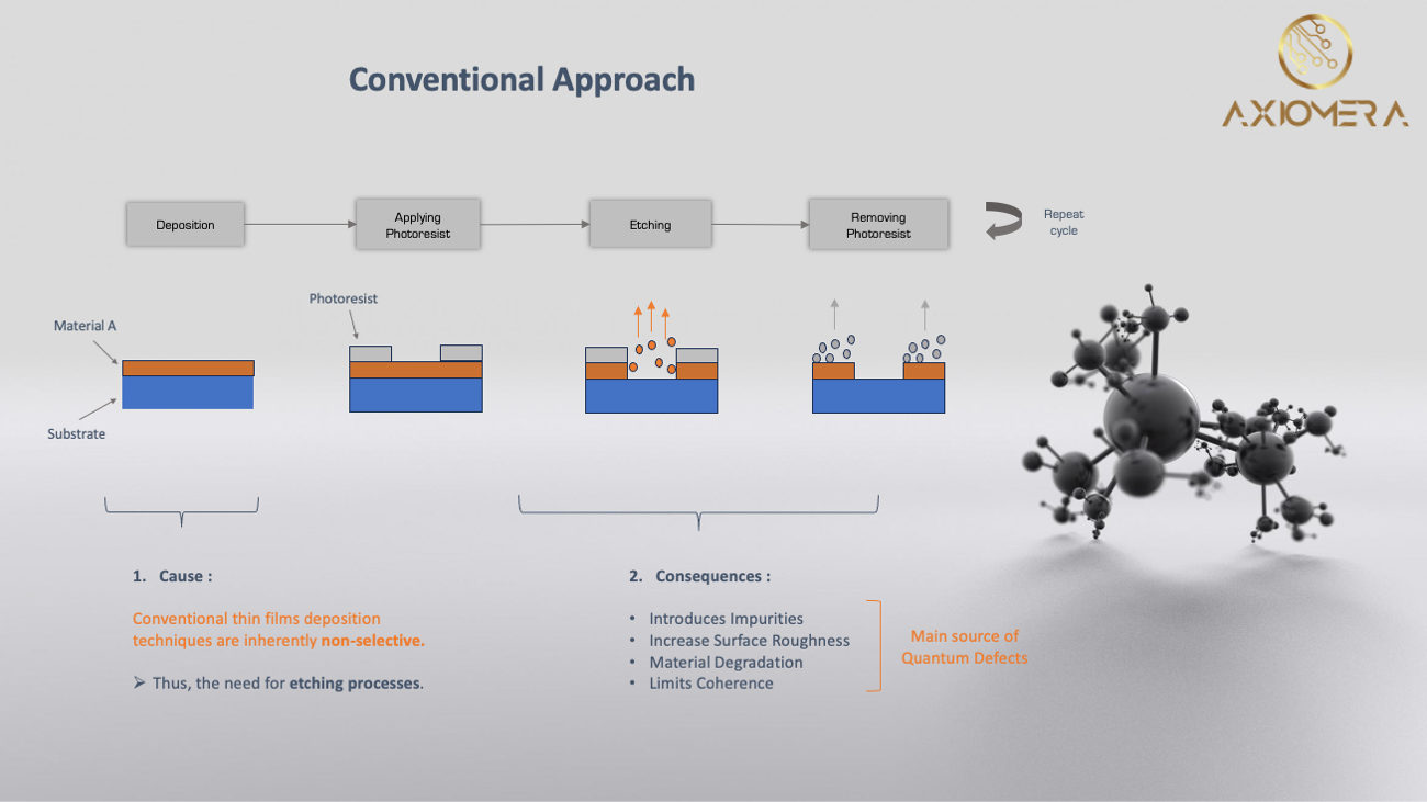
For decades, semiconductor manufacturing has relied on lithography and etching—processes that introduce surface defects, impurities, and variability into materials. While these methods suffice for classical electronics, they pose a fundamental barrier for the next generation of quantum devices.
High-coherence qubits—the building blocks of quantum computers—demand near-perfect material purity and atomic precision. Traditional fabrication techniques fall short:
- Lithography creates rough edges and residual contaminants, leading to decoherence and noise.
- Etching damages surfaces, compromising the integrity of nanoscale structures.
- Lack of 3D control limits the design of complex, defect-free architectures.
These limitations hinder progress across all quantum computing modalities, from superconducting circuits to spin qubits.
Graph: semiconductor manufacturing process overview for material deposition
The Solution: Functional Atomic Layer Deposition (FALD)
AXIOMERA has developed Functional Atomic Layer Deposition (FALD), a breakthrough approach that overcomes the constraints of conventional semiconductor manufacturing while preserving the unmatched precision of ALD.
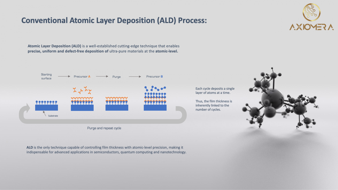
How ALD works?
Atomic Layer Deposition (ALD) is a technique renowned for its:
- Ångström-level thickness control,
- Conformal coating of complex surfaces,
- Ultra-pure material deposition.
Graph: How ALD achieves atomic-scale precision through self-limiting surface reactions.
But FALD goes beyond!
While traditional ALD excels in 2D film deposition, FALD introduces selective, functional control in three dimensions—enabling defect-free, lithography-free fabrication of nanoscale structures. This unique capability allows for:
- Precise material placement without the need for etching or patterning,
- Tailored functionality (e.g., superconductivity, optical properties) at the atomic scale,
- Compatibility with thermal ALD and plasma-enhanced ALD (PEALD), ensuring versatility across applications.
Graph: How FALD achieves Functional control in three dimensions?
The Impact: Enabling High-Coherence Quantum Devices
ALD’s ability to eliminate defects and impurities while enabling 3D functional control transforms quantum device manufacturing. This approach delivers unprecedented coherence and scalability across all major quantum computing platforms:
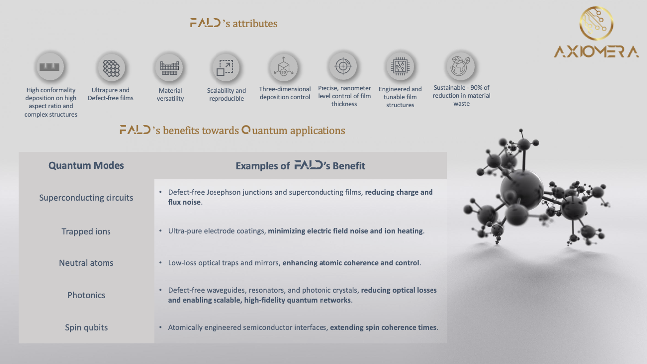
By removing the limitations of lithography and etching, FALD unlocks a new era of performance, reliability, and scalability for superconducting circuits, trapped ions, neutral atoms, photonics, and spin qubits—the five leading approaches in the global race for practical quantum computing.
Sustainability: Revolutionizing Quantum Manufacturing with FALD
Conventional Atomic Layer Deposition (ALD) and other thin-film deposition methods suffer from inherent inefficiencies that undermine sustainability. Traditional ALD coats all surfaces inside the reaction chamber, even though less than 10% of the deposited material is functional. This results in over 90% of rare and costly precursors being wasted as pure byproduct. Additionally, these processes often rely on energy-intensive lithography and etching steps, which generate further waste and require frequent maintenance, including sandblasting, particle trap replacement, and vacuum pump servicing.
In contrast, AxiomEra’s Functional ALD (FALD) technology introduces selective, functional deposition—targeting only the surfaces where material is needed. This precision eliminates the waste associated with conventional ALD and other deposition methods, such as Chemical Vapor Deposition (CVD) or Physical Vapor Deposition (PVD), which often lack the same level of atomic-scale control and material efficiency.
Key sustainability advantages of FALD include:
- Reduced Precursor Waste: By depositing material only on functional surfaces, FALD minimizes the consumption of rare and expensive precursors, directly addressing the 90%+ waste issue of traditional ALD.
- Lower Energy Consumption: Selective deposition reduces the need for energy-intensive subtractive processes like etching or lift-off, aligning with global efforts to lower the carbon footprint of semiconductor manufacturingExtended Equipment Lifespan: FALD’s precision reduces the buildup of unwanted deposits, decreasing maintenance cycles, spare parts replacement, and downtime—further cutting operational costs and environmental impact
- Greener Precursor Chemistry: FALD’s compatibility with optimized, less toxic precursors supports the industry’s shift toward greener chemistry, as highlighted in recent advancements in sustainable ALD processes
Join Us in Shaping the Future
AxiomEra’s mission is to partner with academia, research institutes, and industry leaders to bring this transformative technology to life. Whether you’re exploring fundamental research, device prototyping, or scalable manufacturing, we invite you to:
- Share your perspective on how FALD could advance your work.
- Collaborate on validation, co-development, or early adoption.
- Express formal interest through a Letter of Intent to help shape the future of quantum manufacturing.
Let’s build the next generation of quantum devices—together. Contact us to start the conversation.